TLDR; It’s time to put Canon on your watchlist (ticker: 7751, CAJPY)
Canon has long been the poster child of a large-cap value trap. Its two main businesses — cameras and printers — have faced long-term stagnation. Its stock is trading at the same price as in 2008.
However, things may be finally changing. Dare I say, it might be time for investors to put Canon (back) on the radar.
The key to this shift lies in Canon’s semiconductor business. Wait, semiconductor business? Yes, Canon has quietly maintained an important position in lithography. Only that it has been largely overshadowed by the dominance of the Dutch juggernaut ASML, causing many to overlook Canon’s presence in the field.
While Canon may not be operating at the cutting edge like ASML, it still plays an important role in the industry. Canon’s older deep ultraviolet (DUV) equipment has been experiencing strong demand; last year it sold 187 units (which is over 40% of total units ASML sold), and this year, it’s projected to reach 247 units (+32% YoY).
Older generation equipment are still being used to a great extent, and in fact, their use cases are expanding. For example, Canon’s older i-line technology is finding new applications in back-end chip manufacturing for 2.5/3D advanced packaging — a key process in producing AI chips. Another subtle point is that Canon’s product portfolio focused on older technologies (KrF and i-line) are largely excluded from export restrictions to China, which primarily seeks to block the export of the newer EUV and ArF platforms which Canon does not possess.
While the growth of older generation equipment has been accelerating, the real catalyst for Canon lies in its new nanoimprint lithography (NIL) technology. After two decades of development, Canon began commercializing NIL in 2023. If successful, it offers a viable alternative to conventional photolithography, potentially becoming a game-changer for both the chipmaking industry and also Canon as a firm. The next 3-5 years could be transformative for Canon, putting the stock “back in play”.
In this writeup, we will examine Canon’s history and positioning in lithography, how it stacks up to rivals (ASML, Nikon), Canon’s growth strategies—particularly with the nanoimprint lithography—and, finally, wrapping up with what all of this means for Canon’s stock.
Canon’s history in lithography
Lithography is a process for creating the complex patterns on silicon wafers that form the circuits in electronic devices. Over the past several decades, photolithography, which uses light to transfer these patterns onto wafers, has become the standard in chip manufacturing.
Photolithography was first introduced in chip manufacturing in the 1950s, with the United States leading both the invention and early innovation stages. Foundational work was carried out at Bell Labs and Fairchild Semiconductor. As the semiconductor industry grew in the 1960s and 1970s, Perkin-Elmer and the Geophysics Corporation of America (GCA) emerged as key players, innovating to meet the increasingly technical demands of the field.
The success of American companies did not go unnoticed by Japan. In the 1970’s Japan’s Ministry of International Trade and Industry (MITI) spearheaded a drive to catch up to the US. Japan was successful, and by the 1980s and 1990s, Japan entered a dominant era with Nikon and Canon controlling 75% of the global market for lithography equipment. This dominance extended beyond just lithography, as Japan led across the entire semiconductor value chain.
While the United States and Japan were vying for dominance, a new player was quietly emerging in Europe. ASML was founded in 1984 in the Netherlands as a JV between ASM International and Philips. ASML was a risk taker and through a series of bold technological bets that proved successful, it emerged victorious over the Japanese.
Two innovations stand out as particularly transformative for ASML:
The first was the development of ArF immersion lithography, often referred to as the “wet” process, which introduced a layer of water between the lens and the silicon wafer during the lithography process. This reduced the light’s wavelength, allowing for the creation of finer features. With ArF immersion, ASML secured a decisive advantage over the Japanese, which struggled to keep pace.
The second and most significant was the Extreme Ultraviolet (EUV). This took over 10 years, $25 billion, and the backing of key industry players like TSMC, Samsung, and Intel to bring to market. The technological barrier is so high that ASML has a complete monopoly on EUV equipment, with no other company able to produce it.
When looking back at the evolution of lithography since the 1950’s, what we observe is that industry leadership has shifted every 20-30 years, moving from early inventors like Bell Labs and Fairchild to Perkin-Elmer and GCA, then to Canon and Nikon, and ultimately to ASML (who’s next?) This is a dynamic industry. At one point, ASML itself was a newcomer in the industry. History suggests that there is always a fighting chance for new players, even when incumbents may appear insurmountable.
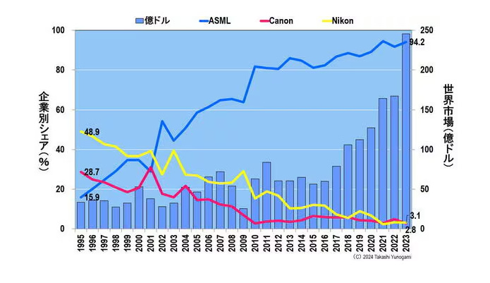
The lithography industry market share from 1995 to 2023 is shown below (chart credit: Takashi Yunogami).
From this chart, one might conclude that ASML has won. That’s correct. However, one might also assume that the Japanese players are no longer relevant in the industry. This would be the wrong conclusion, as we’ll explore next.


